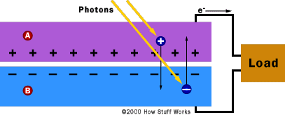
Sunlight is made up of photons, which can be thought of as “packets” of energy (the amount of energy in a photon being proportional to the frequency of its light). When photons strike a solar cell, the vast majority are either reflected or absorbed (some really high-energy photons will blow right through, but they’re of no concern here). When a photon is absorbed, its energy is transferred to the semiconductor — in particular, to an electron in an atom of the cell. If enough energy is transferred, the electron can escape from its normal position associated with that atom. In the process, the electron causes a hole (i.e., an empty spot where the electron used to be) to form. Each photon with enough energy will normally free exactly one electron, and one hole. Note that both electrons and holes are mobile, and as such can be current carriers.

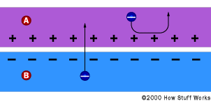
Figure 1. The effect of the electric field in a PV cell (diagram courtesy of How Stuff Works )The simplest solar cells have 3 active layers — a top junction layer (made of
N-type semiconductor ), an absorber layer (a
P-N junction), and a back junction layer (made of
P-type semiconductor). Thanks to the
P-N junction, the cell has it’s own built-in electric field. This electric field provides the voltage needed to force
electrons and
holes freed by light absorption to flow in their own directions (the
electrons to the
N-type side, and the
holes to the
P-type side). If we provide an external
current path,
electrons will flow through this path to their original (
P-type) side to unite with
holes the electric field sent there, doing work for us along the way. The
electron flow provides the
current, and the cell’s electric field causes a voltage. With both
current and voltage, we have power, which is just the product of the two.

Figure 2. Operation of a photovoltaic cell (diagram courtesy of How Stuff Works )After a moment’s thought, you can see that two additional layers must be present in a solar cell –electrical contact layers — to allow electric
current to flow out of and into the cell. The electrical contact layer on the face of the cell where light enters is generally present in some grid pattern and is composed of a good conductor such as a metal. The grid pattern does not cover the entire face of the cell since grid materials, though good electrical conductors, are generally not transparent to light. Hence, the grid pattern must be widely spaced to allow light to enter the solar cell but not to the extent that the electrical contact layer will have difficulty collecting the
current produced by the cell. The back electrical contact layer has no such restrictions — it need simply provide an electrical contact and thus covers the entire back surface of the cell.
Additionally, an antireflective coating is generally applied to the top of the cell to reduce reflection losses, and a cover plate of some kind is often installed to protect the cell from damage while out in the real world.
So now you know. What devices will you run from your solar panels next?
